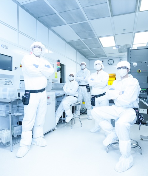
Since 2005, Nanoshift has been a trusted partner in advancing micro- and nano-scale technologies, specializing in wafer level processing for next generation high technology devices and chips. We bridge the gap between prototyping and production by offering comprehensive solutions tailored to the unique needs of each of our clients. Our expertise spans diverse industries and market segments, including private sector, industry, defense, and academia, enabling us to support a wide range of innovative applications.
Our capabilities include Advanced Semiconductor and Advanced Packaging, where we excel in wafer-level packaging, interposers, redistribution layers, and complex architectures such as 3D and 2.5D IC fabrication. With experience in heterogeneous integration of MEMS to CMOS and custom packaging for untraditional or increasing scale applications, we deliver solutions that advance high-technology devices. Through sophisticated process development and scalable methodologies, we ensure smooth transitions from R&D to production while tackling challenges in design, integration, and performance.
In the realm of MEMS, we provide tailored design, development, and fabrication services to fab-less and fab-lite companies. Our expertise supports applications in automotive, consumer electronics, industrial automation, medical devices, and telecommunications, enabling rapid development cycles that reduce entry barriers and accelerate time-to-market. Whether for accelerometers, gyroscopes, RF switches, or diagnostic tools, our MEMS solutions are designed for precision and scalability.
Nanoshift’s work in Microfluidics addresses the needs of life sciences, genomics, medical diagnostics, and lab-on-a-chip applications. Our capabilities include biochips, gene sequencing tools, and cell sorting devices, integrating biocompatible materials with precision fabrication techniques to ensure durability and performance in complex environments. From prototypes to scalable production, we deliver solutions that meet today’s biotechnology demands.
Our Fabrication Processes encompass advanced wafer-level techniques such as photolithography, etching, deposition, planarization, bonding, analysis, and metrology. We work with a variety of materials, substrates, and geometries, offering adaptable process flows that enable high-density packaging, enhanced device performance, allowing for seamless integration with other technologies and applications. Our solutions support the entire product lifecycle, from experimental validation to specialized volume manufacturing.
Unlike traditional foundries that focus on high-volume manufacturing, Nanoshift welcomes projects of all sizes. We deliver the same level of technical insight and commitment to precision for small-scale, iterative prototypes as we do for traditional production. Contact us to learn how Nanoshift’s expertise in Advanced Semiconductor and Advanced Packaging, MEMS, Microfluidics, and Fabrication Processes can help bring your vision to life.